Epitaxial growth (all content)
Note: DoITPoMS Teaching and Learning Packages are intended to be used interactively at a computer! This print-friendly version of the Standalone simulation is provided for convenience, but does not display all the content of the Standalone simulation. For example, any video clips and answers to questions are missing. The formatting (page breaks, etc) of the printed version is unpredictable and highly dependent on your browser.
Contents
Aims
This TLP is designed to help you learn about epitaxial growth; the growth of a (usually thin) single crystalline layer in the same crystallographic orientation as its single crystal substrate. Epitaxial growth is widely used in the electronics industry to enable the deposition of precisely controlled thin layers of semiconductors or oxides for use in devices such as thin film transistors, diodes and lasers.
One of the major film deposition techniques, which is implied in this TLP, is molecular beam epitaxy (MBE). In this technique low energy gas phase beams of atoms or molecules are directed at the crystalline substrate, usually in a vacuum. The resultant thin films are required to be single crystalline and may, or may not, be atomically flat. The exact form of the thin film (flatness, composition, strain, band gap ...) depends sensitively on the growth parameters, of which the most important is temperature.
The aim of this TLP is to allow you to explore the significance of key parameters in the process, such as the substrate temperature and the various bond energies between the atoms involved. At the heart of the package is a two-dimensional simulation of the deposition of the atoms. Using this you can explore the effect of these parameters on the growth of a generic crystal which models many features of "real" systems involving semiconductors such as Si, GaAs and AlGaAs.
The perfection of the thin film depends crucially on the mode of growth of the deposit. Three such modes are usually identified:
- Frank-van der Merwe (one perfect monolayer at a time);
- Volmer-Weber (island growth), and a combination of the two called
- Stranski-Krastanov (one or more perfect layers followed by island growth).
You are encouraged to explore the simulation until you can identify the physical reasons why each of these occurs, and thus the conditions most likely to lead to the preferred growth mode and thin film. Your knowledge will be applicable to other epitaxial growth techniques such as MOCVD and VPE, and not simply MBE.
The questions associated with this TLP should help you to decide whether you have understood the key messages.
Before you start
You can view the epitaxy simulation simply as a rather pretty animation. However in order to fully appreciate what is going on you need to be familiar with the concepts of interatomic bonding, the migration of a single atom across the surface of a crystal (surface diffusion) and the thermal activation of processes (Arrhenius behaviour).
You do not need to know anything specifically about semiconductors or opto-electronics.
Introduction
Epitaxy by MBE involves expensive vacuum deposition equipment such as that shown in the figure.
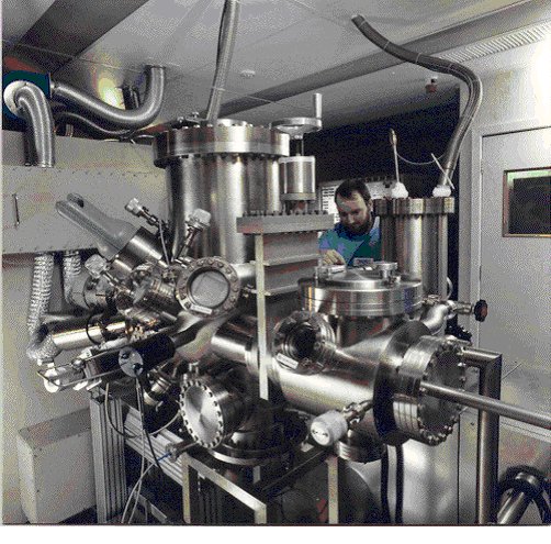
Figure 1 : Epitaxial growth equipment at the University of Liverpool
It is used to deposit thin layers (usually less than a micrometre thick) intended to form the active layers in optoelectronic devices. Such layers must be flat, of precise composition with the appropriate concentration of dopant atoms, and may involve abrupt changes of composition, for instance in order to form quantum wells. The details of the arrangement of the deposited atoms is therefore of great importance: Not only must they adopt the same crystal structure and orientation as their substrate, but the surface of the growing crystal must either be flat or , if not , then rough in a controlled and predictable way.
When the deposited material is of identical composition to the substrate we refer to homoepitaxy, while if the deposit is different from the substrate we refer to heteroepitaxy.
The images in figures 2 and 3 show high resolution TEM images of typical layers, in which the columns of atoms can be seen.
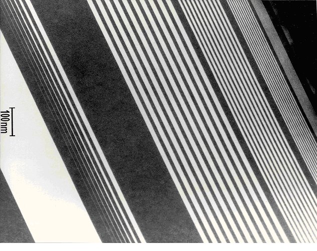
Figure 2 . TEM micrograph of quantum wells in AlGaAs/GaAs imaged so that there is strong contrast between the layers of different composition.
The following image (Figure 3) shows the columns of atoms in alternating epitaxial layers of GaAs and AlAs. The interfaces can be seen to be flat to about one monolayer. The appearance of the AlAs is different from that of the GaAs despite their identical crystal structure because different planes are imaged in the two phases.
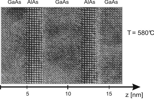
Figure 3 : A high resolution TEM image of alternating GaAs and AlGaAs layers (Simone Montanari PhD thesis (2005))
Figure 4 illustrates the epitaxial growth of a complex compound. The substrate plane is (001) and the heavy atoms show as white dots in a square array. The interface is clearly very flat.
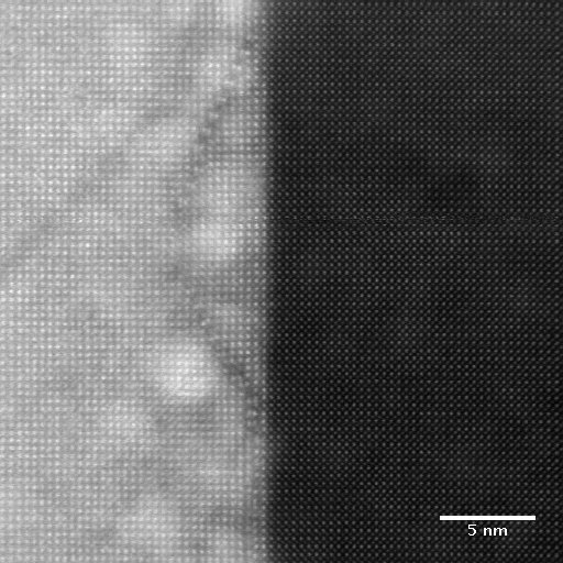
Figure 4: Bi0.5Mn0.5FeO3 film (left hand side, lighter contrast), epitaxially grown on a strontium titanate (SrTiO3 ) single crystal substrate.
The simulation and its limitations
The most obvious limitation of the simulation is its restriction to two dimensions. Surface diffusion on the screen thus only takes place along a line, and atoms are rather more likely to meet each other than in three-dimensional reality. A second less-obvious consequence is that the crystallography of real semiconductors is not reproduced on the screen (silicon and GaAs adopt the "diamond cubic" structure whereas our simulation implies a close-packed fcc structure). Thirdly we have not allowed you to change the rate of production of the deposited atoms. In an MBE reactor this would be controlled via the temperature of the (solid or liquid) sources of gas phase atoms. The simulation must be regarded as a "model" which demonstrates many (but certainly not all) of the behaviours of the real crystals. Another simplification is that the possible existence of impurity or dopant atoms is ignored. This is obviously of huge importance in the device industry, but makes very little difference to the behaviour simulated in this TLP.
However despite all these limitations the model is based soundly on the physics of atomic interactions, and incorporates key aspects of the movement of atoms across surfaces ("surface diffusion") including thermal activation. Atoms will therefore show a greater probability of moving from their original position, across the surface, at higher temperatures. It also takes into account the possibility that the relaxed lattice parameter of the deposited crystal might not be the same as that of the substrate crystal. This often occurs in heteroepitaxy, leading to the build-up of strain in the growing layer. The simulation correctly models many of the behaviours observed during the epitaxial growth of real crystals.
The three common growth modes have the following characteristics:
- Frank-van der Merwe: each layer of deposited atoms is completed before the next layer starts to form. The surface at any instant will be flat or will contain a few monolayer steps.
- Volmer-Weber (island growth): each deposited atom attaches to an island (or incipient particle); islands grow appreciably before joining up to cover the substrate completely. The surface at any instant will not be flat, and the substrate may not be entirely covered.
- Stranski-Krastanov: initially the deposited atoms form one or more perfect layers but this is followed by island growth. The surface is therefore initially flat but develops to become less flat.
Click on this link to launch the epitaxial growth simulation in a new window.
Please note that the simulation is for educational purposes only, and the accuracy of the data contained within it is not guaranteed.
An effective way of using this TLP is to experiment for a few minutes with the simulation, in order to familiarise yourself with its operation, before attempting to answer the following questions, many of which will require that you experiment with the effect of specific variables on the simulated growth, in order to explore different growth regimes. The simulation offers you by default 100 atoms to deposit (three to four atomic layers), but if you need more to see how the film develops, simply increase the number using the slider control.
Notes about the simulation parameters:
- Temperature is shown as Tm, the temperature of the substrate expressed as a fraction of its melting temperature.
- Bond strengths are in arbitrary units on a scale from 0 to 100, where zero implies no bonding and 100 is a strong bond which is unlikely to be broken except at high temperatures.
- Lattice parameter difference is the percentage difference between the natural lattice parameters of the substrate material and the deposit material. If this is non-zero then for epitaxy to occur the deposit must be strained to fit the substrate and therefore strain energy will accumulate as growth occurs.
Summary
After working through this TLP you should understand:
- the importance of growing thin films which are flat at the atomic scale;
- the reasons why three different types of growth can occur during epitaxial deposition;
- the factors which determine the growth mode and hence the flatness of the resultant film;
- the importance of strain in the growth of heteroepitaxial films.
If you read some of the recommended further material (below) you will also appreciate the range of applications for epitaxial films and the existence of alternative growth techniques.
Questions
Click on this link to launch the epitaxial growth simulation in a new window. You may need it to answer some of the questions,
Quick questions
You should be able to answer these questions without too much difficulty after studying this LDP. If not, then you should go through it again!
-
At a medium temperature, say 0.5 Tm, which of these conditions favours layer (Frank-van der Merwe) growth?
Adatom-adatom bond strength Adatom-substrate bond strength Lattice parameter difference -
At a low temperature, say 0.3 Tm, which of these conditions favours island (Volmer-Weber) growth?
Adatom-adatom bond strength Adatom-substrate bond strength Lattice parameter difference -
At a high temperature, say 0.8 Tm, which of these conditions favours Stranski-Krastanov growth?
Adatom-adatom bond strength Adatom-substrate bond strength Lattice parameter difference
Deeper questions
The following questions require some thought and reaching the answer may require you to think beyond the contents of this LDP.
-
At 0.7 Tm, what is the effect of lattice parameter difference in the following cases? Increase the number of atoms from 100 to 150 to see this effect.
Adatom-adatom bond strength Adatom-substrate bond strength Lattice parameter difference
Open-ended questions
The following questions are not provided with answers, but intended to provide food for thought and points for further discussion with other students and teachers.
-
Try to explain the results you saw in the sixteen runs of Questions 1 to 4. Predict a set of parameters which should give Stranski-Krastanov growth at 0.2Tm. e.g. [50, 50, 1]
-
Predict and confirm a set of conditions which might give a gas rather than a deposit [0,0,0] or [0,0,1] at any temperature, because no bonding of adatoms either to substrate or each other]
Deeper questions
The following questions require some thought and reaching the answer may require you to think beyond the contents of this LDP.
-
What happens at 0.5 Tm in the following conditions? Is this physically reasonable?
Adatom-adatom bond strength Adatom-substrate bond strength Lattice parameter difference 100 0 0 -
What happens as more and more atoms are added in the conditions of Q7? What drives this process?
-
Run the simulation with parameters which give you either pronounced SK growth or clear island formation. What shape are the resultant particles or islands?
-
What would you expect to happen to the growing layer if the lattice parameter difference was 5%?
-
If the substrate had been polished so that its surface was not exactly a low-index plane (e.g. perhaps 0.5 degrees away from exact {111}, would there be any occasions during growth when there were no steps on the growing surface?
Going further
Most of the literature relating to epitaxy has arisen in the context of semiconducting or oxide systems. There are currently good articles on Wikipedia which can be found if you search for the following key words:
More on the material covered in this TLP:
- Stranski-Krastanov growth
- Epitaxy
- Molecular beam epitaxy ( don't search for MBE)
For some ideas on why we grow epitaxial thin films:
- Quantum well
- Laser diode
And for some background on other approaches to growth, search for:
- Thin film solar cell
Academic consultant: Peter Goodhew (University of Liverpool), Zoe Barber (University of Cambridge)
Content development: Edd Rowe
Photography and video:
Web development: Lianne Sallows and David Brook
This DoITPoMS resource was funded by the UK Centre for Materials Education and the Department of Materials Science and Metallurgy, University of Cambridge.